Характеристики
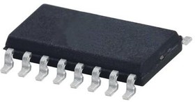
MC14060BDG, Двоичный счетчик со сквозным переносом, 17МГц …The MC14060BDG is a 14-stage Binary Ripple Counter with an on-chip oscillator buffer. The oscillator configuration allows design of either RC or crystal oscillator circuits. Also included on the chip is a reset function which places all outputs into the zero state and disables the oscillator. A negative transition on Clock will advance the counter to the next state. Schmitt trigger action on the input line permits very slow input rise and fall times. Applications include time delay circuits, counter controls and frequency dividing circuits. This device contains protection circuitry to guard against damage due to high static voltages or electric fields. However, precautions must be taken to avoid applications of any voltage higher than maximum rated voltages to this high-impedance circuit. For proper operation, Vin and Vout should be constrained to the range VSS VDD. Unused inputs must always be tied to an appropriate logic voltage level. Unused outputs must be left open.
• Fully static operation
• Diode protection on all inputs
• Buffered outputs available from stages 4 through 10 and 12 through 14
• Common reset line
• Pin-for-pin replacement for CD4060B
 Личный кабинет


 Загрузка