Характеристики
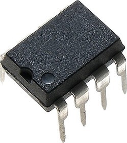
LT1360CN8#PBF, Операционный усилитель, 50 МГц, 1 Усилитель …The LT1360CN8#PBF is a 50MHz high speed high slew rate Operational Amplifier with excellent DC performance. The LT1360 features reduced supply current, lower input offset voltage, lower input bias current and higher DC gain than devices with comparable bandwidth. The circuit topology is a voltage feedback amplifier with the slewing characteristics of a current feedback amplifier. The amplifier is a single gain stage with outstanding settling characteristics which makes the circuit an ideal choice for data acquisition systems. The output drives a 500ohms load to ±13 with ±15V supplies and a 150ohms load to ±3.2 on ±5V supplies. The amplifier is also capable of driving any capacitive load which makes it useful in buffer or cable driver applications.
• 5mA Maximum supply current
• Unity-gain stable
• C-Load™ operational amplifier drives all capacitive loads
• 9nV/√Hz Input noise voltage
• 1mV Maximum input offset voltage
• 1µA Maximum input bias current
• 250nA Maximum input offset current
• 4.5V/mV Minimum DC gain, RL=1k
• 60ns Settling time to 0.1%, 10V Step
• ±13V Minimum output swing into 500R
• ±3.2V Minimum output swing into 150R
• 0.2% Differential gain (AV=2, RL=150R)
• 0.3° Differential phase (AV=2, RL=150R)
• Specified at ±2.5, ±5 and ±15V
 Личный кабинет


 Загрузка